Transducers, gauges, sensors - Information portal © 2011 - 2025 Use of material is possible by placing an active link

Semiconductor strain gauges
Modern semiconductor strain gauges (sensors) on a construction and technical descriptions differ from described below. But principle of work and basic parameters differ small.
Basic materials for making of semiconductor strain gauges presently are silicon and germanium, thus silicon because of his less sensitiveness to the temperature got greater distribution. Semiconductor connections are used also, for example gaas of GaAs and al.
Depending on the applied materials semiconductor strain gauge it is possible to divide into two groups: single-crystal and poly crystalline. Strain gauges, got excision from a single-crystal belong to single-crystal strain gauges; needle-shaped crystals, got growing from a gas phase; epifilms and dendrites. Tenzolity, being artificial mixtures, for example, of coal (or soot) and phenol-formaldehyde lacquer behave to poly crystalline.
Materials for semiconductor strain gauges must possess possibly by the large coefficient of tenzosensitiveness (CTS) and the least temperature coefficient of resistance (TCR), and also to provide stability of parameters of strain gauges.
A very responsible operation at making of semiconductor strain gauges is creation of contact a metal is a semiconductor which turns out of different ways : soldering, fusing in, welding, deposition, electrochemical or chemical causing of coverages.
Certain interest is presented by semiconductor strain gauges from the dendritic web of germanium, getting wide distribution because of simple and accessible technology of making. It is accepted to name the treelike, needle-shaped or as a plate crystals of difficult ambivalent structure, appearing during crystallization in the supercooled fusion or from a supersaturated gas phase dendrites.
Dendritic strain gauges from a germanium differ in the lowered mechanical durability as compared to strain gauges, got from a single-crystal bar. To dignities of dendritic strain gauges it is necessary to take simplicity of making and relative cheapness (as compared to other semiconductor strain gauges dendritic - same cheap). Making germanium dendritic strain gauges does not require the special apparatus (for example, machine-tools for polishing and cutting) and taken to the transversal cutting of dendritic web by a corundum needle, to breaking off of tenzoelement and soldering to him electric conclusions by the special solder. For making of strain gauges a germanium dendritic web is used mainly with specific resistance of r=1±0,2 ohm · of sm. The parameters of such strain gauge strongly depend on a temperature.
Research of strain gauges from a germanium dendritic web allows to educe all features, constrained with the use of semiconductor strain gauges in electric chains.
On structural features semiconductor strain gauges it is possible to divide into glued and unglued. Glued semiconductor strain gauges can be used both with a substrate and unsupported.
Semiconductor strain gauges unsupported differ in the form of section, material and method of realization of ohmyc contact. In a great deal the construction of them is determined by technology of making. The most widespread type of strain gauge is a bar.
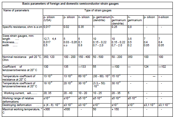
Strain gauges, got growing from a gas phase, there are single-crystal needles by the diameter of 10 - 100 mkm. The construction of such strain gauge with a substrate is shown on a fig. В- 2. The construction of pellicle strain gauge is shown on a fig. В- 2, б; strain gauges is executed as one conducting strip which is covered by the layer of varnish. The parameters of strain gauges are driven to the table.
Basic application semiconductor strain gauges (sensors) find in pressductors, efforts, tensions. Application of semiconductor strain gauges is very perspective in acselerometer.
русский / english
Home >> Mechanical stress, strain >> Semiconductor strain gauges
• Information about various converters and sensors of physical quantities, parameters of various physical processes is presented.
• Electrophysical properties and effects in various electrical materials.
• Theory, experimental results, practical application
Fig. B-2. Design of semiconductor strain gauges: a - strain gauge of needle-like crystals with the substrate, b - film strain gauge


See also:
Work of strain gauge (tensoresistors transducers) is based on property of materials ...
See also:
CONVERTERS, GAUGES, SENSORS
Information, news, advertising