phys. stat. sol. (b) 100, 309 (1980)
Subject classification: 12.2 and 14.3; 22.1.1
Institute of Semiconductors, Academy of Sciences of the Ukrainian SSR, Kiev1)
Piezo Hall Effect in p-Germanium
By
N. T. GORBACHUK, V. V. MITIN, Yu. A. TKHORIK, and Yu. M. SHVARTS
The piezo Hall effect is investigated on p-Ge samples of low (ρ300 K = 0.02 Ωcm) and high (ρ300 K = 16 Ωcm) resistivity in the temperature range 77 to 300 K for the case of current i and uniaxial stress x being parallel to the <100> and <111> crystal axes. Taking into account the dispersion law anisotropy for light and heavy holes allows to explain the experimental temperature dependence of the piezoresistivity coefficients for samples of low and high resistivity and orientational dependence of this effect. The deformation potential constants b and d are obtained which vary in the range b = - (2.2 to 2.6) eV, d = - (4.4 to 5.1) eV depending on the values of the band parameters A, B, and C given in literature. These values of b, d are considerably different from those obtained by means of the same experimental data, but without taking into account the dispersion law anisotropy.
1. Introduction and Formulae for Calculation
The piezo Hall effect in p-Ge has been investigated in [1, 2]. However, the dispersion law anisotropy (DLA) was not taken into account in the calculations and thus in the interpretation of the experimental results. Taking account of the DLA influences sufficiently the results of the piezoresistivity calculation (see, for example, [3]). There-fore, it is of interest to consider this influence on the piezo Hall effect, too.
The dependence of the Hall coefficient upon the value of the uniaxial stress X is determined by the expression
(1)
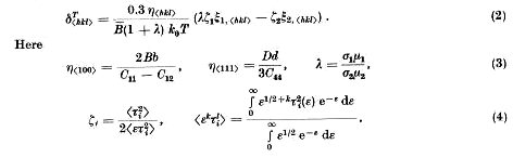
where R0(μ1σ1 + μ2σ2)/[c(σ1 + σ2)] ; μi; σi are the Hall mobility and conductivity for the light (i = 1) and heavy (i = 2) holes, respectively, δ<hkl> + 1/2π<hkl> is the piezo Hall effect coefficient, π<hkl> is the longitudinal piezoresistance coefficient, δ<hkl> = δ0<hkl> + δT<hkl> , δ0<hkl> are temperature independent and δT<hkl> are temperature dependent components of δ<hkl>.
For the interpretation of the experimental results only δT<hkl> are used. The expres¬sion for δT<hkl> may be easily obtained according to [4]
Transducers, gauges, sensors - Information portal © 2011 - 2025 Use of material is possible by placing an active link
Home >> Publication, literature >> Piezo Hall Effect in p-Germanium
русский / english
• Information about various converters and sensors of physical quantities, parameters of various physical processes is presented.
• Electrophysical properties and effects in various electrical materials.
• Theory, experimental results, practical application
ε ist the hole energy in k0T units, B = √ B^2 + C^2/5, B, D, C are the valence band constants [4]. In (2) only the parameters ξi,<hkl> depend on DLA. Their analytical expression is written in the Appendix because it is cumbersome. It follows from the Appendix that the neglect of DLA gives = 1 while taking into this circumstance leads
to the deviation of ξi,<hkl> from unity.
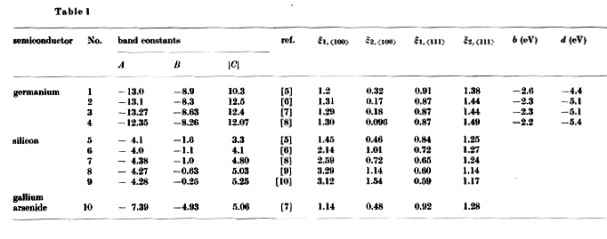
We calculated ξi,<hkl> using the formulae of the Appendix and different sets of constants A, B, and C which are known [5 to 10] for p-Ge, p-Si, and p-GaAs. The results are listed in Table 1. It is seen from the table that the parameters ξi,<hkl> for Ge slightly differ from one set to another due to a slight distinction of the different sets of constants A, B, and C. Quite another situation takes place in Si, for which the scatter of values A, B, and C is large.
2. Experimental Results and Comparison with Calculation Data
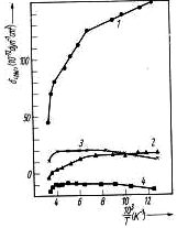
Samples of p-Ge of resistivity ρ300 K = 16 Ωcm and ρ300 K = 0.02 Ωcm and sizes of 0.7 X 0.7 X 8 mm^3 were investigated. The long dimension of samples coincided with <100> or <111> directions. The dependence of R and ρ on X was measured under small loads (in the region of linear dependence of these values on the stress) in the temperature range from 77 to 300 K for i || x || <100> and i || x || <111> directions (i is the current vector). π<hkl> = (ρx - ρ0)/ρ0X and δ<hkl> +1/2 π<hkl> = (Rx - R0)/R0X (i.e. experimental dependence of δ<hkl> on temperature) were determined (see Fig. 1). It is seen from Fig. 1 that in the relatively pure semiconductor (curves 1 and 2)
Fig. 1. Temperature dependence of δ<100> ((1) and (3)) and δ<111> ((2) and (4)) in p-Ge. (1) and (2) ρ300 K = 16 Ωcm, (3) and (4) ρ300 K = 0.02 Ωcm
δ<100> and δ<111> are positive and increase with rising 1/T. This indicates the predominating contribution of light holes to δ<hkl> — see (2). Supposing λ = 2.8, ζ1 = 1 (this is correct, if the scattering on acoustic phonons is predominant), C44 = 6.67 x 10^11 dyn per cm^2, C11 — C12 = 8.02 X 10^11 dyn/cm2 [11]. After that we obtain the values of the deformation potential constants (see Table 1) from a comparison of theoretical and experimental slopes δ<hkl>(1/T) for the region where δ<hkl> depends linearly on 1/T.
By neglecting DLA ( ζi,<hkl> = 1) b and d are quite equal for the all sets of band parameters listed in Table 1 (b ≈ —4.4 eV, d ≈ —2.8 eV). These values are considerably different from b and d obtained by us with taking into account of DLA. Moreover this result (|b| > |d|) is in contradiction to literature data [12]. Therefore, it is necessary to take into account DLA in the interpretation of the experimental results. Especially it must be noted that in contrast to the case i || x || <100> for which λξ1,<100> >> ξ2,<100> and the contribution of the light holes is principal, the value ξ2,<111> is close to λξ1,<111> for i || x || <100>. That is why the difference λξ1,<111> — ξ2,<111> is very sensitive to the choice of the λ value. In particular, if λ is smaller than 1.52; 1.66; 1.71, and 1.66 for the first, second, third, and fourth sets of constants, respectively, this difference has always another sign.
The slope of δ<hkl>(1/T) for a heavily doped semiconductor is practically zero at temperatures larger than 120 K (curves 3, 4). This is caused by decreasing of ζi and λ (for scattering on ionized impurities ζi = 1/9, λ ≤ 0.36). Although the slopes of curves 3 and 4 are small, it should be noted that they have different signs. This may be explained by predominant contributions of heavy holes to δ<111> and light holes to δ<100> for λ≤ 1 (see (2)). The slope of the δ<hkl>(1/T) curves changes in the sample with ρ = 0.02 Ωcm, if T < 120 K. This is caused by the transition to another conductivity mechanism. In this temperature range R has a maximum and the reduction of R with decreasing temperature indicates a contribution of hopping conductivity [13].
3. Conclusion
Comparing the values of b and d obtained with taking into account DLA and without it, we come to the following conclusion.
It is necessary to take into account CLA in the interpretation of the piezo Hall effect in p-Ge (in particular, in the experimental determination of the deformation potential constants). This circumstance allows to account for the experimentally observed features of the piezo Hall effect in p-Ge and to obtain reasonable estimations for the deformation potential constants b and d.
The accuracy of determination of the deformation potential constants is limited by the precision with which the band parameters A, B, and C are known. In Si, where the scatter of values A, B, and C is large, the corresponding scatter of values ξi,<hkl> is large, too. This creates difficulties for the determination of b and d.
Acknowledgement
The authors wish to thank A. Yu. Tkhorik for performing the numerical calculations
References
[1] M. INOUE and M. IKEDA, J. Phys. Soc. Japan 20, 1542 (1965).
[2] G. E. PiKUS and G. L. BIR, Fiz. tverd. Tela 1, 1.828 (1959).
[3] G. L. Bir, A. I. BLOOM, and V. V. ILISAVSKY, Proc. VII. Internat. Conf. Phys. Semicond., Paris 1964 (p. 529).
[4] G. L. Bir and G. E. PIKUS, Simmetriya i deformatsionnye effecty v poluprovodnikakh, Nauka, Moskva 1972.
[5] G. DRESSELHAUS, A. F. KIP, and C. KITTEL, Phys. Rev. 98, 368 (1955).
[6] B. LAX and J. MAVROIDES, Solid State Phys. 11, 261 (1960).
[7] I. M. TSIDILKOVSKII, Zonnaya structura poluprovodnikov, Nauka, Moskva 1978.
[8] F. POLLAK and M. CARDONA, Phys. Rev. 142, 530 (1.966).
[9] I. BALSLEV and P. LAWAETZ, Phys. Letters 19, 6 (1965).
[10] J. HENSEL and G. FEHER, Phys. Rev. 129, 1041 (1963).
[11] H. J. Mc SKIMIN and P. ANDREATCH, J. appl. Phys. 35, 3312 (1964).
[12] P. I. BARANSKII, V. P. KLOCHKOV, and I. V. POTYKEVICH, Poluprovodnikovaya elektronika, Naukova dumka, Kiev 1975 (p. 6).
[13] B.I. SHKLOVSKII and A. L. EFROS, Elektronnye svoistva legirovannykh poluprovodnikov, Nauka, Moskva 1979 (p. 109).
(Received February 1980)


See also:
CONVERTERS, GAUGES, SENSORS
Information, news, advertising