Transducers, gauges, sensors - Information portal © 2011 - 2025 Use of material is possible by placing an active link
русский / english
Home >> Magnetic field >> Sensors are a hall - effect
• Information about various converters and sensors of physical quantities, parameters of various physical processes is presented.
• Electrophysical properties and effects in various electrical materials.
• Theory, experimental results, practical application
Home >> Magnetic field >> The Hall Sensor. The principle of operation of physical processes

We assume that the free charge carriers in the plate are electrons, and they provide the conductivity of the plate. In the absence of a magnetic field the electrons move in an electric field E of the voltage source under the force of Coulomb (Fk = eE, e is the charge of an electron) is generally straightforward in the direction of the positive electrode (against the direction of the electric field E voltage source in the plate) (Fig.2). After the appearance of the magnetic field B moving with velocity V, the electrons start to act the Lorentz force (Fl = eVB), and change their trajectory bringing it closer to the circle, deflecting the electrons towards one of the faces of the plate (Fig.3). The deviation of the electrons occurs until then, until the Coulomb force field Hall Fx does not counterbalance the Lorentz force Fl.
Thus, near one of the edges of the plate accumulates an excessive amount of electrons, it is negatively charged relative to the opposite face. An electric field Ex (field Hall) and, accordingly, the electrical contacts of the opposite faces of the Hall voltage Ux (EMF Hall) (Fig.4).
Analyzing kinetic phenomena in the disc we can obtain a formula determining the voltage of the Hall:
ε x ≈ Ux = A/ne • IB/d, (1)
where the coefficient A ≈ 1 ÷ 2 (depend on the dissipation mechanisms), n is concentration of charge carriers, I is the current, d is the thickness of the plate.
Analysis of formula (1) shows that almost the main parameter which determines the sensitivity of the Hall sensor (γ = ΔUx/ΔB) is the mobility of carriers μ (I = μne). Therefore, the sensing elements of the Hall sensors made from semiconducting materials: InSb, GaAs, Si, Ge. Some mobility can reach tens of thousands cm2/V•s.
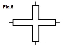
The sensing elements of the Hall sensors are manufactured in various shapes of plates with four pads and electric insights. The shape of the plate may be different. Most often, cross-shaped (Fig.5). The sizes of the records influence the sensitivity, linearity. Therefore, the size of optimize when designing the sensor. Typically, the length of the sensing element is not less than three times the width.
Currently used in the manufacture of microelectronic planar technology that allows you to create sensing elements with the size of the workspace on the level of 100x100 µm. The sensitivity of modern Hall sensor can reach several thousand mV/T.
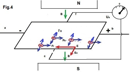
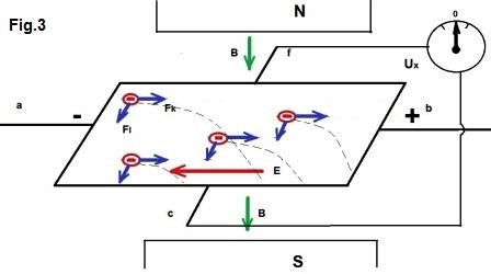
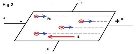
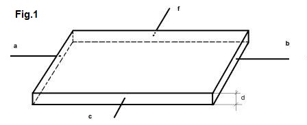
The physical processes that lead to the Hall effect can be demonstrated using the following figures Fig. 1-4.
The Hall Sensor. The principle of operation of physical processes
The Hall sensor is called a magnetoelectric device based on the Hall effect and which is mainly intended for measurements of magnetic fields, as well as to create different transducers using electromagnetic fields.
The Hall effect is that when a conducting plate (Fig.1) with a current in a magnetic field in the plate in the direction perpendicular to the current of an electric field and, accordingly, the voltage - Hall voltage (EMF Hall). Effect named after the scientist Edwin Hall who discovered the effect.
See also:
CONVERTERS, GAUGES, SENSORS
Information, news, advertising
