Transducers, gauges, sensors - Information portal © 2011 - 2025 Use of material is possible by placing an active link
Semiconductor lasers . Laser on the p- n junction
In an intrinsic semiconductor conduction band electrons are always thermally abandoned from the valence band. When light passes through a semiconductor, electrons from the valence band absorb light quanta and transferred to the conduction band , if the frequency of the incident light
ν ≥ Еg/h
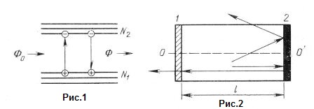
(Eg - band gap, h- Planck's constant). Consequently, the intensity of light decreases by passing through the semiconductor. Simultaneously, the radiation incident on the semiconductor stimulated transitions of excited electrons from the conduction band to the valence band. In this light quanta emitted (Fig. 1 . ). These photons are added external radiation as it passes through the semiconductor, ie, there is an amplification of light.
Transitions occurring under the influence of external radiation, called induced in contrast to spontaneous transitions occurring independently of external radiation. At thermodynamic equilibrium, the number of electrons in the valence band is many times greater than in the conduction band. Consequently, the absorption of light prevails over gain. For light amplification is necessary to create conditions under which the concentration of electrons near the bottom of the conduction band is greater than the concentration of near the valence band (N2> N1). Such a state is called the state of the semiconductor with a population inversion levels.
Gain a light as it passes through the semiconductor depends on the difference between the populations of the upper and lower levels. Since the probabilities of transitions up and down electrons are equal, then the amplification occurs when the population difference of the upper and lower levels of N2-N1> 0.
By weakening the light passing through a semiconductor lead not only transitions from the valence band to the conduction band , but the scattering of light at different crystal inhomogeneities. As a result, the intensity of light varies with the distance x into the semiconductor by law
Ф = Ф0ехр(α - χп)х,
where the coefficient cop characterizes losses. Thus, the semiconductor chip enhances the external radiation, if it has a population inversion and the gain exceeds the loss factor (α > χп).
In order to turn the amplifier radiation generator, you must enter a positive inverse relationship, ie, part of the radiation output from the input file. In lasers to create feedback working crystal is placed between two parallel mirrors (1 and 2 in Fig . 2). Light passing through the crystal will increase in exp(α - χп )l times, then reflected from the mirror, will be held again and again through the crystal will increase by the same amount, etc. The primary light quanta are due to spontaneous transitions, and then there is an amplification of light propagating in the crystal due to induced transitions.
It should be noted that an amplifier with a positive feedback loop may become a generator only when the gain exceeds all radiation losses in the device. It is therefore necessary to consider the loss introduced by the feedback device, ie mirrors. Upon reflection from the mirror, the light intensity decreases again in R where R - reflectance.
Population inversion of the semiconductor can create many methods. One of them is an intrinsic semiconductor irradiated by intense light ( optical pumping). The electrons move from the valence band to the conduction band, and accumulate there. At a sufficiently high pump intensity may occur population inversion levels. Another method is to transfer electrons from the valence band to the conduction band of the semiconductor bombardment by fast electrons. With both methods, you can receive large radiation power, but overall efficiency of devices is small.
Greatest efficiency and simplicity of design has a laser on the p -n- junction. Consider, for example, the most widespread construction of the laser on the p -n- transition of gallium arsenide. Laser action is based on the fact that a forward bias electrons are injected into the p region where they are radiative recombination with existing holes there. To create a state with a population inversion requires more concentration of holes in the valence band, which is achieved by increasing the concentration of the acceptor impurity doping. In order to injection of electrons into the p region exceed the injection holes in the n-region (where nonradiative recombination, and consequently, the hole current in the n- region belongs entirely to the loss ), it is necessary that the concentration of the donor impurity in the n- region has higher concentration of acceptor impurities in the p- region, ie, пп>рр.
Thus, to obtain the status of a population inversion in the p-region requires a high degree of doping of both regions p -n- junction.
Consider the difference between LED radiation from the laser diode . In the LED is spontaneous emission, ie, different parts of the emitting region emit independently. As a result of the lighting source emits waves propagating in all directions , and the light intensity is inversely proportional to the square of the distance from the source.
In the laser optical cavity through the use of all light waves are directed at an angle to the axis of the active area, either immediately or after several reflections are deflected away from the axis of the resonator and are not amplified. Furthermore, the laser radiation is produced as a result of a coordinated induced electron transfer from the conduction band to the valence band in the entire radiating part of the p-region, so the spatial coherence ( ie, direction ) is maintained across the output beam cross section of light.
Best material for laser diodes is currently gallium arsenide. The thickness of the radiating portion of the p-region of the order of 2 microns. The laser diode is a first laser, which succeeded in the direct conversion of electrical energy into coherent optical radiation. It also has the highest efficiency and highest performance. Laser diodes may be used in light locators for observation and photographing in the dark in a range finders as well as for communication, because they are extremely easy to carry out modulation of light emission change of the amplitude or frequency of the supply voltage.
Although theoretically the efficiency of laser diodes can be close to 100%, practically it is much smaller. The main reason - the need for heavily doped p-n and n- junction regions. Simultaneously with the introduction of impurities into a semiconductor, a large quantity of defects in the active region, which leads to considerable losses of radiation. Moreover, defects may form energy levels in the forbidden band of the semiconductor. Because the concentration of impurities in both sides of p -n- transition is large, the width of the p -n- transition is small, and consequently the carriers from the conduction band can move on these levels, then the valence band to tunnel into the p-region. The tunneling current is not associated with radiation, and it also degrades efficiency.
Due to these reasons for the occurrence of stimulated emission requires a large threshold current density. The large current density through the p -n- junction degrade the parameters of laser diodes, but also to the need for bulky cooling system. Therefore, the total quantum yield at room temperature of not more than 2 ... 3%. The threshold current density of the order of 10 ^ 4 A/cm2. Degradation of radiation parameters associated with the current flow of high densities. Thus there is a migration of atoms (ions) of uncontrolled impurities and the formation of new defects in the emitting region. All of them increase the number of nonradiative recombination centers and reduce efficiency, which also leads to an increase in the surface recombination velocity and the leakage current on the surface. When working at the maximum of the radiation power may occur a crack in the active region of the laser resonator mirrors and deteriorate.
References: I.M.Vikulin, V.I.Stafeev. Physics of semiconductor devices. MA - 1990
Fig.1. Interband transitions under the action of radiation on the semiconductor.
Fig.2. Scheme semiconductor laser.
русский / english
Home >> Photo effects, light >> Semiconductor lasers . Laser on the p- n junction
• Information about various converters and sensors of physical quantities, parameters of various physical processes is presented.
• Electrophysical properties and effects in various electrical materials.
• Theory, experimental results, practical application


See also:
CONVERTERS, GAUGES, SENSORS
Information, news, advertising