Transducers, gauges, sensors - Information portal © 2011 - 2025 Use of material is possible by placing an active link
Design gate photocells
In principle, the construction of all cells with a barrier layer is the same . In each particular case, of course, there may be certain differences, but they do not change the overall nature of the construction of the photocell. Can only change the shape of the photocell, its dimensions, methods of the upper electrode, the output of such electrodes, etc.
Usually valve manufacture solar cell begins with the so-called lower electrode - metal plate thickness of 1-2 mm, on which a thin layer of semiconductor. Then, the semiconductor layer is treated to create in it thicker p -n- junction. Thereafter, the outer surface is applied in most cases the upper metal electrode which is a thin semi-transparent metal layer, light transmissive.
Sometimes the processing to create a semiconductor layer of p -n- transition is performed when the upper metal already deposited electrode. There are cases in the absence of semiconductor processing both electrodes. The latter are created after formation of the semiconductor layer in the p -n- junction. In some photocells p -n- junction is formed during the deposition of the upper electrode.
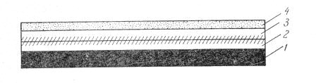
Thus, the photocell valve includes a lower metal electrode, the electron (or hole ), a semiconductor layer, a barrier layer, the hole (or electron ) layer, an upper metal translucent electrode ( Fig. 1).
Photocell is placed in a plastic mandrel with a window for light. In mandrel strengthened two current terminals, one connected to the bottom, the other - with the top electrode. To protect the outer surface of the solar cell from the harmful effects of air sometimes it is covered with a transparent varnish. Some types of solar cells are placed in a small glass flask from which the air is pumped out , or whether it is filled with some inert gas.
If Photocell made of highly conductive semiconductor material such as silicon or germanium, the upper electrode may be formed as a ring if the photosensitive surface is shaped disc or rectangle. Of course, there may be other solutions.
Incident on the solar cell surface radiant flux reflected from the partially translucent, and a metal electrode partially absorbed therein. Part of the flow passing through the electrode is absorbed in the adjoining semiconductor layer. As a result, this layer having a pair of electron - hole. Electrons are concentrated at the electrode covering the semiconductor layer, which electronic conduction mechanism, and the hole - hole on the electrode of the semiconductor. Between the lower and the upper electrode there is a potential difference, whose value is up to a certain limit will be the greater, the greater the intensity of the radiant flux. Electrodes hooked photocell external circuit, we will create the conditions for the occurrence of an electric current in it. So it will be until the photocell is illuminated, the light in the range of small streams with the limit value of 1 lumen solar cell short-circuit current is almost linearly dependent on the light intensity. When the photocell is an external circuit resistance, this linearity is broken.
In recent years, physicists have concentrated on getting the PV of new materials with a large integral sensitivity. At the same time represent additional challenges - as much as possible to extend the spectral response of the photocell that he felt not only the entire visible spectrum, but also perhaps more invisible - infrared and ultra violet.
Increased sensitivity and integral extension of the spectral characteristics of the solar cell are of paramount importance. Do photocell feeling significant infrared and ultraviolet region of the spectrum would be very wide range of applications in various fields of engineering. Photocells such does not exist, therefore understandable struggle for the expansion of the spectral characteristics of the solar cell toward the infrared part of the spectrum as the temperature light sources send radiation, which is the maximum energy in the infrared region.
Ica photoelectric processes in photovoltaics gate, have a noticeable lag, which affects the shape of their frequency characteristics. This inertia arises mainly due to the fact that solar cells have their own gate capacitance is much greater than the capacity of cells with external photoeffect. Therefore, at the drop of the valve AC photocell light flux with some frequency, a current depends on this frequency: the frequency increases, the photocurrent decreases. The nature of this decrease is different for different solar cells.
Strong reduction of the impact of the majority gate photocells with increasing frequency limits their use in the case of alternating light fluxes relatively high frequency, such as sound film. However, despite the sluggishness, a few years ago sernotallievye solar cells have been successfully used for sound reproduction in some Leningrad theaters.
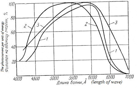
Valve photocells made of different photosensitive semiconductor materials. Widespread selenium photocells. Spectral characteristic of a selenium photocell is close to the sensitivity of the human eye, the maximum spectral sensitivity is in the range 5500-6000 A (0,55 - 0,6 μm), ie lies. the visible part of the spectrum ( Fig. 2). Integral sensitivity of selenium photocell is 600 μA / lm, ie, greater than the sensitivity of photocells external photoeffect.
Still more prevalent photocells of silver sulfide (Ag2S) - FESS. The integral sensitivity of FESS reaches 9000 µa/LM, rather broad spectral response (from 0.4 to 1.4 μm) with high sensitivity in the near infrared region of 0.8 to 0.9 μm). Semistationary solar cells have high stability in operation.
русский / english
Home >> Photo effects, light >> Design gate photocells
• Information about various converters and sensors of physical quantities, parameters of various physical processes is presented.
• Electrophysical properties and effects in various electrical materials.
• Theory, experimental results, practical application
Fig . 1. Schematic structure of the valve photocell: 1 - bottom metal electrode, 2 - electron (hole ) semiconductor layer, 3 - hole (electron ) semiconductor layer, 4 - upper metal semitransparent electrode. The shaded area - the barrier layer.
Fig. 2. Spectral description of selenium photocell. 1 - pure selenium, 2 - selenium mixed with sulphur, 3 - selenium with tellurium impurity


See also:
CONVERTERS, GAUGES, SENSORS
Information, news, advertising