Transducers, gauges, sensors - Information portal © 2011 - 2023 Use of material is possible by placing an active link


русский / english
Home >> Publication >> Study of some properties of electrophysical n-Si, alloy ion implantation
• Information about various converters and sensors of physical quantities, parameters of various physical processes is presented.
• Electrophysical properties and effects in various electrical materials.
• Theory, experimental results, practical application


Study of some properties of electrophysical n-Si, alloy ion implantation
Introduction
Electrical properties of semiconductors may not only depend on the dopant type and concentration, but also on the method of doping, which leads to a particular impurity distribution in space technology and other related effects to a certain extent influence the parameters. Silicon used in practice is conventionally divided into three classes: uniformly doped, diffusion and ion- implanted / 1 /. Published data indicate that the least studied the electrical properties of ion- implanted silicon.
Silicon is very widely used in strain measurement and authors mainly interested tensosensitivity ( piezoresistive effect), the resistivity and temperature dependence in ion-implanted silicon layers .
Theoretical analysis
For the general case, when the direction of the stress σ and current density j are arbitrary angle, piezoresistive effect in semiconductors with a cubic lattice theoretically described using piezoresistive πij or elastorezistivnyh mij coefficients , which are fourth-rank tensor / 1, 2 /. These factors are linked through pliability coefficients and moduli of elasticity. For crystals of the symmetry class to which it belongs silicon crystallographic axes in the system to describe the piezoresistive effect is enough to know three factors: π 11, π12 and π44, sometimes called the main piezoresistive coefficients. Primary piezoresistive coefficients depend on many factors: the material, the conductivity type, resistivity, the doping level, temperature, mechanical strain (stress).
In / 3.4 / for example, shows the known combinations of the piezoresistance coefficients in directions stress and current density coinciding with a certain crystallographic axes.
All three main piezoresistance coefficient can be determined by measurements in three different directions / 3, 4 /. Full tensor piezoresistance πijkl is defined as follows:
where σkl - stress tensor, Δρij - resistivity tensor. It is known that the stress tensor is a symmetric tensor and has six independent components. The same is true for the resistivity tensor.
With that said in the six-dimensional space can be obtained by:
For bulk n-Si alloying and uniform ρ = 11.7 ohm- cm at work / 5 / results obtained: π11 = -102.2, π12 = 53.7, π44 = -13.6.
In the layers of silicon diffusion alloyed piezoresistive coefficients determined by the concentration of the impurity on the surface layer Nn / 6 / and practically do not depend on the distribution of impurities. Results obtained in the same study results show that for the n-Si ratio π11 at room temperature varies from 17x10^-11 m2 /Nm ( Nn = 1x10^21 cm- 3) to 88x10^-11 m2 /Nm ( Nn = 1.8x10^18 cm -3). Marked temperature dependence π11 starts with Nn = 9x10^19 cm -3 ( about 0.1% / K).
It should be noted that due to the peculiarities of the band structure of n-Si for not very high degree of doping of silicon valid assumptions / 5 /:
π44 ≅ 0; π11 ≅ -2 π12
As the concentration of impurities occurs violation of these assumptions that need to be considered. For diffusion layers violations occur when Nп ≥ 5x10^19 cm-3 /1, 6/.
Experimental part
We investigated by ion implantation of phosphorus doped polycrystalline thin film on the n- Si (100) plane of monocrystalline silicon with the insulating layer SiO2. Such structures may be more manufacturable using planar fabrication technologies transmitters.
Experimentally measured resistivity ? Coefficients longitudinal kII = ΔρII/ρII·εII ( where ΔρII - change the resistivity along the direction of deformation εII), and transverse k⊥ = Δρ⊥/ρ⊥·εII ( where Δρ⊥ - Change the resistivity perpendicular to the direction of deformation εII) Gage, piezoresistance coefficients πII = (π11 + π12 + π44)/ 2 и π⊥ = (π11 + π12 - π44)/ 2 , and deformation temperature dependence of these quantities.
Films pre pared on the ( 100 ) silicon. The film thickness was 0.6 micrometers, the dopant concentration of 5x10^18 cm -3. Resistivity of 0.013 ohm cm measurements were performed on samples of size 8x0.6x0.4 mm film on the surface.
Piezoresistance coefficients of measurement carried out as with the console steel beams of equal resistance to bending and by direct sample loading. In measurements using beams, and using the amount of deformation calculated from the known formula
εб = hδ / lб^2
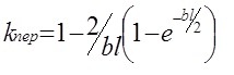
(where h - the thickness of the beam lb - beam length, δ - movement of the free end of the beam ) were obtained coefficients Gage бkII (ε II <110>; J II <110>) and бk⊥ (ε II <110>; J ⊥ <110>) -27,3 and -2,8, respectively. However, such measurements may be used in the calibration of strain gauges , and for research into the physical properties of the film need to know immediately its deformation (stress). As known / 7 / are not all transmitted from the beam deformation to the sample . Transmitted deformation depends on the size of the sample , the elastic properties of the sample and the binder , whereby the sample is attached to a beam . Accounting for this effect can be made using transmission factor whose value (for the case when the target is in the center of the film specimen) we determined according to the formula / 8 /:
wherein, , G - shear modulus binder, E - elastic modulus sensing element ( sample ), Q - sectional area of sample, , h - the thickness of the sample, hc - the thickness of the binder, l - length of the sample.
Substituting the parameters of our measurement conditions ( for hc = 0.15 mm ) obtain kпер = 0.68. Taking into account the transmission coefficient and calculating the true strain εо = εб x kпер gearbox under study film obtain the actual values of the coefficients Gage films kII = -40,1 and k⊥ = -3,8.
When measuring gage by direct loading sample was mounted cantilever and bending load was applied . Measurement error coefficients by this method did not exceed 4 %. At room temperature the following values πII = -24,9 and π⊥ = -2,4.
If we consider the elastic properties of silicon used in our crystallographic orientation of the sample and recalculate obtained using beams gauge factor k in the piezoresistance coefficients π ( considering the ratio σ =Eε, where E - modulus of elasticity ε - relative deformation ), we find that the difference in values π measured in many ways, does not exceed 6 %. In our view, this suggests good accuracy formulas for kпер / 8 / and the need to consider factor, especially when the size of the samples exceeding the thickness of the binder. It should be noted that is important in determining the correct values hc and G formula.
Fig .1 shows the results of measurements of the temperature dependenceπ and ρ, and in Fig. 2 shows the relationship ρ from longitudinal stresses. The temperature dependence of the resistivity is 0.08 % / K, and Gage 0.15% / K.
Compared with the bulk silicon and diffusion layers of the same doping level / 1, 3, 6 / piezoresistance coefficients corresponding investigated films are close to them in size, but the temperature dependence of the parameters below for the films doped by ion implantation. The difference may be due to more homogeneous and polycrystalline doped.
Conclusion
Thus, studies have shown that ion- doped polycrystalline silicon layers with comparable with other types of silicon strain sensitivity are less temperature dependent parameters. In the study using gage beams must be taken into account a transfer efficiency of sample deformation. In the future, we plan to conduct research for various doping levels, types of conductivity, crystallographic orientation.
REFERENCES
1. Vaganov V.I. Integral tenzopreobrazovatel. -M . Energoatomizdat, 1983. - 136.
2 . Thurston R. Application of semiconductor converters for measuring strain , acceleration and displacement. - In.: Physical Acoustics / Ed. W. Mason, Volume 1, Part B, Methods and tools for ultrasound. Lane. from English. - New York: Wiley, 1967, p.187 -209.
3 . K. Seeger, Semiconductor Physics. Lane. from English. ed. JK Pozhela. -M. : Mir, 1977, p. 615.
4 . Smith C.S. Phys. Rev., 1954, 94, c. 42.
5 . Smith C.S. Piezoresistance effect in germanium and silicon. - Phys. Rev. 1954, v. 94, 1, p. 42-49.
6. Tufte O.N., Stelzer E.L. Piezoresistive properties of silicon diffused lauers. - J. Appl. Phys., 1963, v. 34, 9, p. 313-318.
7. Fouretier G. La Dynamometrie de Precision / / Analyse des Contraintes. - 1957 , v. 11, 9-10, p. 19-27.
8. Klokova N.P. Gages: Theory, methods of calculation, design. - M.: Mechanical Engineering, 1990. -224 With.
Gorbachuk N.T., Didenko P.I.. Research of some electrophysics properties of tapes of n - Si alloyed by ionic implantation. Surface, 2006, 4, p. 104-106.
See also:
CONVERTERS, GAUGES, SENSORS
Information, news, advertising